Services/PCB Design
PCB Design & Circuit Board Layout
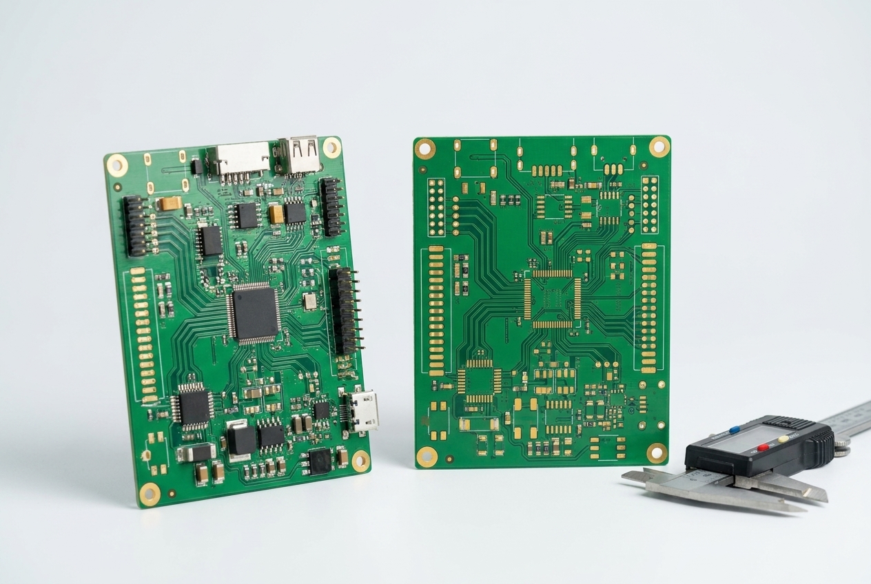
SiGenix is a contract PCB design firm providing full-cycle printed circuit board design services — schematic capture, component selection, multi-layer PCB layout, signal integrity analysis, and manufacturing documentation. Whether you need a custom PCB design from scratch or an experienced PCB layout engineer to take over an existing board, we deliver mixed-signal, high-speed, and RF designs from concept to fabrication-ready Gerbers.
From Concept Schematic to Fabrication-Ready Board
Good PCB design starts long before layout. We begin with careful component selection and schematic capture, thinking through power architecture, signal integrity, thermal paths, and manufacturability while the design is still cheap to change.
Our engineers have laid out boards from simple 2-layer designs to dense 16+ layer stackups with impedance-controlled high-speed routing. Every design ships with complete fabrication documentation — Gerbers, drill files, assembly drawings, and a design-for-manufacturability review — so your board house and assembler can build it right the first time.
What Our PCB Design Services Include
Schematic Capture & Component Selection
Circuit design and schematic capture with careful component selection — balancing performance, cost, availability, and lifecycle so your board can actually be built and kept in production.
Multi-Layer PCB Layout
Board layout from 2 to 16+ layers, including dense mixed-signal designs, fine-pitch BGA fanout, and layer stackup planning for signal integrity and EMI performance.
High-Speed Signal Integrity
Signal integrity analysis and impedance-controlled trace routing for high-speed digital interfaces — length matching, differential pairs, and termination strategies.
Thermal & Power Plane Design
Thermal management and power distribution design — copper pours, thermal vias, and plane strategies that keep components within ratings under real load.
Fabrication Documentation
Complete manufacturing packages: Gerbers, NC drill files, fabrication notes, and assembly documentation ready to hand to any board house.
Design for Manufacturability
DFM review before release — footprint checks, clearances, panelization, and assembly considerations that prevent expensive respins.
Frequently Asked Questions
Can you take over an existing PCB design?
Yes. We regularly pick up designs started elsewhere — reviewing the schematic and layout, fixing signal integrity or EMI problems, and carrying the board through to production-ready documentation.
How complex a board can you lay out?
We design boards from simple 2-layer designs to 16+ layer stackups, including high-speed digital interfaces, impedance-controlled routing, fine-pitch BGAs, mixed-signal partitioning, and RF front-ends.
Do you design with EMI compliance in mind?
Yes. EMI-aware layout is built into our process — stackup planning, partitioning, return path management, and filtering — so boards pass radiated and conducted emissions testing without late redesigns.
Do you support the board through manufacturing?
Yes. Every design includes fabrication-ready Gerbers, assembly documentation, and a design-for-manufacturability review, and we can assemble and bring up first-article prototypes in-house.
Have a board that needs designing?
Whether it's a new design from scratch or an existing board with problems, describe what you're building and we'll tell you honestly how we can help.
Contact Us